The difference between thin and thick film make this a natural choice.
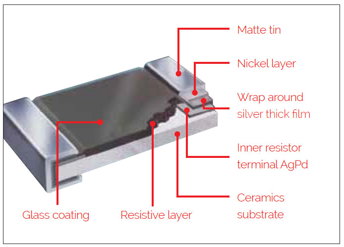
The construction of Riedon’s CRW and CRS series of thick film chip resistors with galvanic nickel barrier layers. They feature matte tin terminations.
It is recommended to use thin film technology rather than thick film for 0.1% tolerance or better high precision products for better resistance consistency. From the perspective of product structure, the biggest difference between thick and thin film is the material type and manufacturing method of the resistance layer. A thick film resistor is manufactured using a process similar to silk-screening. The product consistency and stability are far less than than that of a thin film resistor.
Thin film resistors apply resistance alloy in a very thin film formed on a ceramics substrate by using vacuum deposition to create a resistance layer with less than 1μm in thickness. Thick film resistors, on the other hand, form the resistance layer on ceramics substrate by applying printing resistance ink with 5~10μm thickness; that is why it is called thick film. Because of the increased thickness of the resistance material with the thick film process, laser trimming methods can vary greatly and this will also affect other characteristics of the product. In general, the characteristics of thin film resistors are focused on high precision, low TCR, and long term stability.